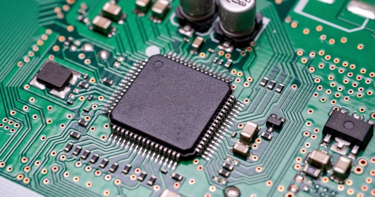
Printed Circuit Boards (PCBs) are the fundamental building blocks of modern electronics, serving as the connective tissue that allows electronic components to function cohesively. From the simplest gadgets to the most complex industrial machinery, PCBs are indispensable. The evolution of electronics demands increasingly sophisticated PCB solutions, pushing manufacturers to innovate in areas like miniaturization, signal integrity, and thermal management. This article delves into the intricate world of PCB fabrication and Printed Circuit Board Assembly (PCBA), exploring the technical expertise required to produce high-quality boards and the advanced solutions that are shaping the future of various industries.
The Foundation: Understanding PCB Fabrication
PCB fabrication is a multi-step process that transforms a design into a physical circuit board. It begins with a substrate material, typically fiberglass reinforced epoxy (FR-4), onto which conductive pathways are etched. The complexity of this process varies significantly depending on the type of PCB being manufactured. Single-sided PCBs are the simplest, featuring conductive traces on only one side. Double-sided PCBs, as the name suggests, have traces on both sides, connected by plated through-holes. Multilayer PCBs, however, represent a significant leap in complexity, incorporating multiple layers of conductive material separated by insulating layers, all laminated together under high pressure and temperature. This layered approach allows for much denser circuitry and improved performance, crucial for today’s compact and powerful electronic devices.
The fabrication process involves several critical stages, each requiring precision and specialized equipment. These include:
•Design and Pre-production: This initial phase involves converting the electronic design into manufacturing data, including Gerber files, which define the copper layers, solder mask, and silkscreen. Design for Manufacturability (DFM) checks are performed to identify and resolve potential issues before production begins.
•Material Preparation: The core material, often FR-4, is cut to size. For specialized applications, other materials like Rogers laminates (for high-frequency applications) or aluminum substrates (for thermal management) may be used.
•Inner Layer Imaging: For multilayer PCBs, the inner copper layers are cleaned, coated with a photoresist, and exposed to UV light through a phototool. The exposed photoresist hardens, protecting the copper that will form the circuit traces. The unexposed photoresist is then removed, and the unprotected copper is etched away.
•Layer Lamination: The etched inner layers, along with prepreg (a bonding material) and copper foil, are stacked and laminated together under intense heat and pressure. This process creates a solid, multilayer board.
•Drilling: Holes are drilled through the laminated board. These holes serve various purposes, including vias (for electrical connections between layers), component leads, and mounting holes. Precision drilling is paramount to ensure proper alignment and connectivity.
•Plating: After drilling, the inside of the holes and the surface of the board are chemically plated with a thin layer of copper. This process, known as electroless copper deposition, creates conductive paths through the vias and prepares the surface for further etching.
•Outer Layer Imaging and Etching: Similar to inner layer imaging, photoresist is applied to the outer layers, exposed, and developed. The exposed copper is then etched to form the final external traces and pads.
•Solder Mask Application: A protective layer of solder mask is applied over the copper traces, leaving only the pads exposed for soldering. This prevents solder bridges and protects the circuitry from environmental factors.
•Surface Finish: A surface finish is applied to the exposed copper pads to prevent oxidation and improve solderability. Common finishes include Hot Air Solder Leveling (HASL), Electroless Nickel Immersion Gold (ENIG), and Organic Solderability Preservative (OSP).
•Silkscreen Printing: Component designators, logos, and other markings are printed onto the board using silkscreen.
•Electrical Testing: Each board undergoes electrical testing to ensure continuity and isolation, verifying that all circuits function as designed.
•Routing and Finishing: Finally, the individual PCBs are routed out from the larger panel, and any necessary finishing operations, such as beveling or scoring, are performed.
See also: Communication Challenges in Technology
The Art of PCB Assembly (PCBA)
Once the bare PCB is fabricated, the next crucial step is Printed Circuit Board Assembly (PCBA). This involves populating the board with electronic components, transforming it into a functional electronic module. PCBA requires a blend of automated processes and skilled manual labor, especially for complex boards or specialized components. The primary methods of assembly are Surface Mount Technology (SMT) and Through-Hole Technology (THT), often used in combination (MIX assembly).
Surface Mount Technology (SMT)
SMT is the dominant assembly method for most modern electronics due to its ability to place small components rapidly and accurately. Surface Mount Devices (SMDs) are designed to be directly mounted onto the surface of the PCB, eliminating the need for through-holes. The SMT process typically involves:
1.Solder Paste Application: Solder paste, a mixture of tiny solder spheres and flux, is precisely applied to the component pads on the PCB using a stencil printer.
2.Component Placement: Automated pick-and-place machines accurately position SMDs onto the solder paste. These machines can place thousands of components per hour with high precision.
3.Reflow Soldering: The populated board passes through a reflow oven, where controlled heating melts the solder paste, forming strong electrical and mechanical connections between the components and the PCB pads. The temperature profile in the oven is critical to prevent damage to components and ensure proper solder joint formation.
4.Inspection: After reflow, the boards undergo various inspection methods, including Automated Optical Inspection (AOI) and X-ray inspection, to detect defects such as missing components, incorrect placement, or poor solder joints.
Through-Hole Technology (THT)
THT involves inserting component leads through holes drilled in the PCB and then soldering them on the opposite side. While less common for high-density boards, THT is still used for larger, heavier components, connectors, or components that require greater mechanical strength. The THT process typically involves:
1.Manual or Automated Insertion: Components are either manually inserted into the through-holes or placed by automated insertion machines.
2.Wave Soldering or Manual Soldering: For wave soldering, the board passes over a wave of molten solder, which solders all the component leads simultaneously. Manual soldering is used for specific components or for rework.
3.Inspection: Similar to SMT, THT boards are inspected for proper component placement and solder joint quality.
Mixed Technology Assembly
Many modern electronic devices utilize both SMT and THT components, requiring a mixed technology assembly approach. This often involves performing SMT processes first, followed by THT processes, to optimize efficiency and quality.
Advanced PCB Solutions: Pushing the Boundaries
The demand for more powerful, compact, and reliable electronic devices has driven the development of advanced PCB solutions. Two prominent examples are Rigid-Flex PCBs and High-Frequency PCBs, each addressing specific challenges in electronic design.
Rigid-Flex PCBs: Combining Strength and Flexibility
Rigid-Flex PCBs integrate the best features of both rigid and flexible circuit boards. They consist of multiple layers of flexible circuits connected to rigid PCBs, forming a single, interconnected unit. This hybrid design offers several significant advantages:
•Space Savings: Rigid-Flex boards can be folded or bent to fit into irregular or constrained spaces, eliminating the need for connectors and cables, thereby reducing overall system size and weight.
•Enhanced Reliability: By reducing the number of connectors and solder joints, Rigid-Flex PCBs minimize potential points of failure, leading to increased reliability and durability, especially in applications subjected to vibration or shock.
•Improved Performance: The shorter signal paths and controlled impedance offered by Rigid-Flex designs can lead to better electrical performance and signal integrity.
•Simplified Assembly: Integrating multiple boards and cables into a single Rigid-Flex unit simplifies the assembly process and reduces manufacturing costs.
Rigid-Flex PCBs are widely used in demanding applications such as aerospace, medical devices, military equipment, and high-end consumer electronics where space, weight, and reliability are critical factors.
High-Frequency PCBs: For Speed and Signal Integrity
High-Frequency PCBs are specifically designed to handle signals in the gigahertz range, crucial for applications like 5G communication, radar systems, satellite technology, and high-speed data networking. The challenges in designing and manufacturing high-frequency boards stem from the need to maintain signal integrity, minimize signal loss, and control impedance at very high speeds. Key considerations for High-Frequency PCBs include:
•Material Selection: Standard FR-4 materials can exhibit significant signal loss at high frequencies. Therefore, specialized low-loss dielectric materials, such as Rogers laminates, are often used to minimize signal attenuation and maintain stable dielectric properties.
•Controlled Impedance: Maintaining a consistent impedance throughout the signal path is vital to prevent reflections and signal distortion. This requires precise control over trace width, dielectric thickness, and material properties.
•Trace Geometry: Short, smooth traces with minimal bends and discontinuities are preferred to reduce signal degradation. Differential pair routing is commonly employed to improve noise immunity.
•Grounding and Shielding: Effective grounding schemes and shielding techniques are essential to minimize electromagnetic interference (EMI) and crosstalk.
The meticulous design and fabrication of High-Frequency PCBs ensure that high-speed signals are transmitted with minimal loss and distortion, enabling the performance required by advanced communication and data processing systems.
Applications Across Industries
The technical expertise in PCB fabrication and PCBA manufacturing, particularly in advanced solutions like Rigid-Flex and High-Frequency PCBs, finds critical applications across a diverse range of industries:
•Telecommunications: The rollout of 5G networks and the continuous demand for faster data transmission rely heavily on High-Frequency PCBs for base stations, antennas, and networking equipment. These boards ensure the integrity of high-speed signals, enabling reliable and efficient communication. Furthermore, complex telecommunication equipment often benefits from the space-saving and reliability advantages of Rigid-Flex PCBs.
•Robotics: Robotics, encompassing industrial automation, service robots, and drones, requires highly reliable and compact electronic systems. Rigid-Flex PCBs are ideal for robotic applications due allowing for intricate wiring in confined spaces and providing robust connections that can withstand constant movement and vibration. The ability to integrate multiple functions into a single board simplifies robotic designs and enhances their agility and performance.
•Automotive: Modern vehicles are increasingly reliant on sophisticated electronics for engine control, infotainment systems, advanced driver-assistance systems (ADAS), and electric powertrains. PCBs in automotive applications must withstand harsh environments, including extreme temperatures, vibrations, and humidity. High-Frequency PCBs are crucial for radar and sensor systems in ADAS, while Rigid-Flex PCBs contribute to compact and reliable electronic modules throughout the vehicle.
•Medical Devices: Precision, reliability, and miniaturization are paramount in medical electronics. From implantable devices to diagnostic equipment, PCBs must meet stringent quality standards. Rigid-Flex PCBs enable the creation of smaller, more flexible, and more reliable medical devices, while specialized PCBs ensure the accurate functioning of sensitive diagnostic instruments.
•Industrial Control: Industrial automation systems, including programmable logic controllers (PLCs), motor drives, and sensor networks, demand robust and reliable PCBs that can operate continuously in challenging industrial environments. The ability to handle high power and complex signal processing is essential for these applications.
Partnering for Excellence in PCB & PCBA Manufacturing
Choosing the right manufacturing partner is paramount for businesses seeking to leverage advanced PCB and PCBA solutions. A reputable manufacturer offers not only state-of-the-art fabrication and assembly capabilities but also deep technical expertise, stringent quality control, and comprehensive support throughout the product lifecycle. They should be proficient in handling diverse PCB types, from standard rigid boards to complex Rigid-Flex and High-Frequency designs, and offer end-to-end services from design validation to final assembly.
For companies looking for a reliable partner in advanced PCB and PCBA manufacturing, consider the comprehensive services offered by Global Well PCBA. With a focus on technical excellence and a wide range of advanced PCB solutions, they cater to the demanding requirements of industries such as telecommunications and robotics, ensuring high-quality and innovative electronic products.
Conclusion
The world of electronics is continually evolving, driven by the relentless pursuit of innovation. At the heart of this evolution are Printed Circuit Boards, which continue to become more sophisticated and specialized. From the foundational processes of PCB fabrication and assembly to the cutting-edge advancements in Rigid-Flex and High-Frequency designs, the expertise required to produce these critical components is immense. As industries like telecommunications and robotics push the boundaries of technology, the role of advanced PCB and PCBA manufacturing will only grow in importance, enabling the next generation of electronic devices and systems. Understanding these complexities and partnering with experienced manufacturers is key to success in today’s rapidly advancing technological landscape.